The board is designed around a LATTICE iCE40UP5K that implement a ATmega32U4 with the necessary IO's to run unmodified arduboy games, also ( optionally ) includes a VS1053b audio decoder to play music from uSD or create games with more complex sounds.
This board is a derivation of ARDUFPGA ICE40UP5K V1.1 board
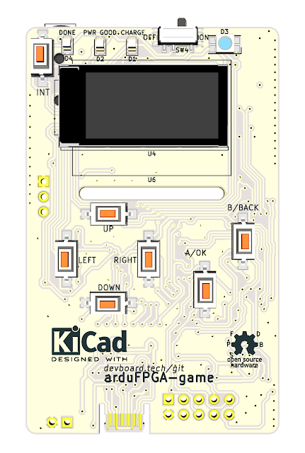
in portable format with a size of only 68x43mm, smaller than a credit card.
As hardware, there is:
1x LATTICE iCE40UP5K.
1x SSD1306 OLED 128x64 BW display/ ST 7735S 160x80 color TFT display.
1x 2MB of SPI FLASH for the design, the GUI boot-loader and the user application (game), with an endurance of minimum 100K erase/write.
1x Optionally VS1053b dedicated audio decoder.
1x Electret buzzer.
1x RGB powerfull LED that can be used as flashlight without exiting the played games.
1x Dedicated battery charger with status LED's.
Design and firmware's:
Games and applications are load from a uSD card thru two stage boot-loader:
The first stage that is written inside the design and has its own 2KBytes of ROM memory and 512Bytes of RAM memory, it has even a dedicated interrupt vector named NMI that interrupt the running game every 1mS and check for INT button to be pressed, this is the service function that check if the INT button is press, if INT button is press between 100mS and 500mS this function will load the GUI boot-loader, if is press more than 500 mS will disconnect the keyboard from the running application and run the alternate functions.
Second stage is a GUI explorer/boot-loader that is loaded into the emulated ATmega32U4 program memory running like a normal application or a game and has integrated the FAT FS library, check and update the design and GUI boot-loader every time a game or application is launch, in case if the running design is custom made for that application or game, when the game or running application is interrupted the GUI boot-loader will automatically save the EEPROM content to the uSD card, and load the EEPROM content from uSD card when a game or application is started, so, all game scores and history is saved if the game is changed.
At this moment all games are in binary format, need to be converted from hex to bin files in order to run.
The design has the capability to increase the size of ROM and RAM memory according to each developer necessities, but no more than 128KB combined.
Different designs, applications source code,boot-loaders source code, user guides, schematic's and other stuff will be available on:
https://github.com/dev-board-tech
Of course, design and application ideas are very welcome.
Update:
If you short press the INT button ( between 100mS and 500mS ) the game is interrupted and the EEPROM content is saved to the uSD memory.
If you press INT button more that 500 milliseconds, the keyboard is disconnected from the application, and buttons have other functionalities done by the first stage boot-loader that runs like a bios in background.
The features of the first stage boot-loader are:
- INT+ B button change the LED colour B,G,R.
- INT+ A button turn ON/OFF the flashlight (RGB led becomes flashlight).
- INT+ UP increase the game volume in four steps, from mute to maximum.
- INT+ DN decrease the game volume in four steps, from maximum to mute.
- INT+ DN decrease the game volume in four steps, from maximum to mute.
- INT+ LEFT switch the USB connector function between UART RX/TX and video NTSC composite output.
- INT+ RIGHT switch the audio connector function between audio and video NTSC composite output, as protection to avoid driving the audio connector by VS10xx and the FPGA, when VS10xx is out of reset the audio connector can not be switch to composite output.
All this functionalities at the same tame when you playing games or listen music.
The volume mostly has effect on headphones, the electret buzzer does not react to much to the volume change, the volume is changed using two four bit PWN generators in the design that are connected to PORTA bit [3:2], bit [3:2] of the PWM are connected to '0' and bit [1:0] to PORTA, the real maximum volume is 1/4 of total power to avoid blowing up the listener ears :slight_smile: .
The audio connector is connected directly to VS1053b and three pins of the FPGA, this pins are used by the game as audio outputs but alternatively can be used as data communication, one of the pins needing to be put to '0' to provide the ground for the communication.
The USB type C connector is used for charging the battery, and for data communication, eight pins of the FPGA are wired to this connector, six of them are divided in three pairs of two wires that can be used for fast differential bidirectional communication and and are match between them or can be used as general purpose IO's, and two that can be used as general purpose IO's.
There is another 3 pin header named ONE-WIRE header.
BW version SSD1306:
Color version: ST 7735S:
The current design is a reduced IO, ATmega32u4 compatible core with 64KB of emulated FLASH memory and 32KB of RAM memory, TIM0, TIM3, TIM4, SPI, UART ( incomplete ), emulated EEPROM, extra-reduced PLL ( USB clock generator strip away ), 10bit LFSR RNG as ADC.
System IO's:
* PIOA used for design FLASH chip select, application FLASH chip select. external chip select on the ARDVARK connector, and volume control as outputs, all seven keys and LoBat signal as inputs.
* Ports 0xDB-0xFF used for boot status and FLASH memory write registers.
The external chip select on the ARDVARK connector can be used as CS for an external SPI device connected to ARDVARK connector and in case if the user brick's the arduFPGA console to recover it using any other arduFPGA console or a regular SPI programmer.
Board consumption from the battery is 29mA with the display at maximum bright ~90% of the pixels active, uSD initialized, RGB LED OFF, and VS1053b in reset mode ( no consumption ).
The board is smaller than a credit card only 68x43x10mm in size and the space in the back of the board close to audio connector can be glued a battery up to 1Amp's in capacity giving a huge game play/ music listen time for one charge.
Here is a demo: